Integrated circuit IC
FBelec is a leading stocking distributor of Obsolete, Hard to Find, and Active Integrated Circuits.
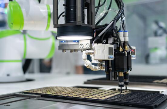
Our total commitment to quality and exceeding customer expectations has made us a true leader in the electronic distribution industry. Below is a catalog of Integrated Circuits. To locate the exact part you are looking for, please use our part search utility or, contact us and a sales associate will be more than happy to assist you . Commonly known as ICs or chips. These chips contain a vast number of electronic components, such as transistors, resistors, capacitors, and interconnects, which are interconnected to perform specific functions. The fabrication process in the factory involves the creation of these complex IC designs on the silicon wafer using advanced techniques and machinery.
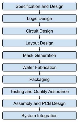
IC Design and Manufacturing Process Steps
Integrated circuit (IC) design and manufacturing process involves several steps to create complex electronic circuits on a small semiconductor chip.
IC Design and Manufacturing Process
IC Design and PCB Design Compared
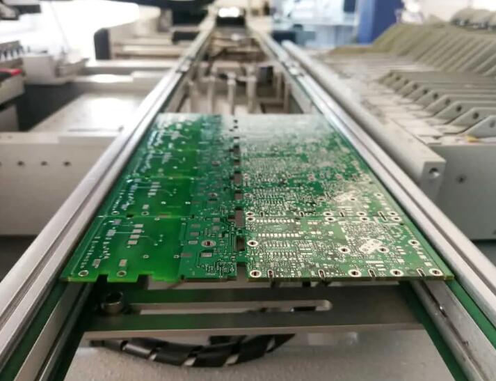
IC design and manufacturing involve creating intricate circuitry on a silicon chip, while PCB design focuses on designing the physical board that incorporates ICs and other electronic components, facilitating their interconnections and integration into a more extensive system. While related, they represent different aspects of electronic design and production.
The steps in the PCB design process include the following
Schematic Design: The PCB design process begins with capturing the schematic of the electronic circuit using a schematic capture tool. Components are selected and interconnected to represent functionality.
Component Selection: Components are selected and sourced for the PCB assembly based on the schematic. Factors such as availability, cost, footprint, and electrical characteristics are considered.
PCB Layout Design: The layout design involves translating the schematic into a physical PCB layout. It includes component placement, routing of traces, and creation of power and ground planes. The layout is optimized for signal integrity, manufacturability, and thermal management.
Design Rule Check: Once the PCB layout is complete, a design rule check is performed to ensure compliance with manufacturing constraints, such as clearances, minimum trace widths, and minimum drill sizes.
Gerber Generation: The PCB design files, including the copper layers, solder mask, and silkscreen, are exported in the Gerber format, the industry standard for PCB manufacturing.
Prototyping and Testing: A prototype PCB is manufactured and assembled with the selected components. The assembled PCB is tested for functionality, electrical performance, and reliability.
Manufacturing: After the prototyping phase, the PCB design files are sent to a fabrication facility where the PCBs are produced in bulk. Manufacturing involves drilling, plating, solder mask application, and component assembly.
Integrated circuit (collectively referred to as semiconductor component products)
Integrated circuit , after the invention and mass production of transistors, various solid-state semiconductor components such as diodes and transistors have been widely used to replace the functions and roles of vacuum tubes in circuits. By the middle and late 20th century, the progress of semiconductor manufacturing technology made integrated circuits possible. Compared with manually assembled circuits using individual discrete electronic components, integrated circuits can integrate a large number of microcrystalline tubes into a small chip, which is a great progress. The scale, production capacity, reliability and modular method of circuit design ensure the rapid adoption of standardized integrated circuits instead of discrete transistors.
Integrated circuits have two main advantages over discrete transistors: cost and performance. The low cost is because the chip prints all components as a unit through photolithography technology, rather than making only one transistor at a time. The high performance is due to the fast switching of components, which consumes less energy because the components are small and close to each other. In 2006, the chip area ranged from a few square millimeters to 350 mm, Per mm It can reach a million transistors.
The first prototype of integrated circuit was completed by Jack Kilby in 1958. It includes a bipolar transistor, three resistors and a capacitor.
According to the number of microelectronic devices integrated on a chip, integrated circuits can be divided into the following categories:
Small scale integration (SSI) has less than 10 logic gates or less than 100 transistors.
There are 11 ~ 100 medium scale integration logic gates or 101 ~ 1K transistors.
There are 101 ~ 1K logic gates or 1001 ~ 10K transistors in large scale integration (LSI).
Very large scale integration (VLSI) has 1001 ~ 10K logic gates or 10001 ~ 100k transistors.
There are 10001 ~ 1m logic gates or 100001 ~ 10m transistors in ULSI.
Glsi (full English Name: Giga scale integration) has more than 1000001 logic gates or more than 10000001 transistors.
Classification of IC
There are many classification methods of integrated circuits. According to whether the circuit belongs to analog or digital, it can be divided into analog integrated circuits, digital integrated circuits and mixed signal integrated circuits (analog and digital are on one chip).
Digital integrated circuits can contain anything, from thousands to millions of logic gates, flip flops, multitasking and other circuits on a few square millimeters. The small size of these circuits enables higher speed, lower power consumption (see low power design) and lower manufacturing cost compared with board level integration. These digital ICs, represented by microprocessors, digital signal processors and microcontrollers, use binary to process 1 and 0 signals.
Analog integrated circuits, such as sensors, power control circuits and operational amplifiers, process analog signals. Complete the functions of amplification, filtering, demodulation and mixing. By using analog integrated circuits with good characteristics designed by experts, the burden of circuit designers is reduced, and there is no need to design everything from the basic transistors.
Integrated circuits can integrate analog and digital circuits on a single chip to make devices such as analog-to-digital converters and digital to analog converters. This circuit provides smaller size and lower cost, but care must be taken for signal collision.
IC model
The chip naming method is generally: letter + number + letter
The first letter is the abbreviation of chip manufacturer or a chip family. For example, most of the MC starts with Motorola, and most of the max starts with Meixin.
The number in the middle is the function model. Like mc7805 and lm7805, it can be seen from the 7805 that their function is to output 5V, but the manufacturers are different.
The following letters are mostly packaging information. You can know what packaging the specific letters represent only by looking at the data provided by the manufacturer.
74 series is the common name of standard TTL logic devices, such as 74ls00, 74ls02, etc. we can't see what company's products are from 74 alone. Different companies will prefix 74, such as sn74ls00.
Related development semiconductor integrated circuits
Generally, a complete IC model must include at least the following four parts:
Prefix (initial) - many can speculate which company's products are.
Device name -- generally, the function of the product can be inferred (its capacity can be known from memory).
Temperature grade ---- distinguish commercial grade, industrial grade, military grade, etc. Generally, C represents civil grade, I represents industrial grade, e represents extended industrial grade, a represents aviation grade and M represents military grade.
Package -- indicate the package and pin number of the product, and some IC models will have other contents:
Rate -- for example, memory, MCU, DSP, FPGA and other products have rate differences, such as - 5 and - 6.
Process structure -- for example, general digital IC has COMS and TL, which are commonly represented by letters C and t.
Environmental protection - generally, there will be a letter at the end of the model to indicate whether it is environmental protection, such as Z, R, +, etc.
Packaging - displays the packaging in which the material is transported, such as tube, t / R, rail, trail, etc.
Version number - displays the number of modifications of the product. Generally, M is the first version.
IC naming, packaging common sense and naming rules:
Temperature range
C = 0 ℃ to 60 ℃ (commercial grade); I = - 20 ℃ to 85 ℃ (industrial grade); E = - 40 ℃ to 85 ℃ (extended industrial grade); A = - 40 ℃ to 82 ℃ (aviation grade); M = - 55 ℃ to 125 ℃ (military grade)
Package type:
A—SSOP; B—CERQUAD; C-to-200, TQFP; d-ceramic copper top; E—QSOP; F-ceramic SOP; H-sbgaj-ceramic dip; K—TO-3; L—LCC,M—MQFP; N -- narrow dip; n -- dip;; Q—PLCC; R - narrow ceramic dip (300mil); S—TO-52,T—TO5,TO-99,TO-100﹔U—TSSOP,uMAX,SOT; W-wide body small appearance (300mil); x-sc-60 (3P, 5p, 6p); y-narrow body copper top; Z—TO-92,MQUAD; D - bare sheet/ PR - enhanced plastic packaging; / W - wafer.
Number of pins
A—8; B—10﹔C—12,192; D—14; E—16; F——22,256; G—4; H—4; I—28 ; J—2; K—5,68; L—40; M—6,48; N—18; O—42; P—20﹔Q—2,100﹔R—3,843; S——4,80; T—6,160; U—60; V-8 (round); W-10 (round); x-36; Y-8 (circular); Z-10 (circular).
Note: if the first letter of the four letter suffix of interface products is e, it means that the device has anti-static function
Copyright © 2021 NINGBO FBELE ELECTRONICS CO.,LTD. All Right Resrved Designed by www.followala.com
Welcome to text me on WhatsApp or send me an email to sales@fbelec.com